SureView has developed an automated inspection system for Semi-conductor wafers (chips) based on Machine Vision.
Based on our competency in test & measurement of over 4 decades, we have developed this equipment in India for manufacturers of semi-conductors. This system consists of a high resolution frame-grabber, synchronized illumination, machine vision algorithm and other allied accessories.
This equipment is made to:
- Detect & Record the Wafer ID (using optical character recognition)
- Detect & Quantify Scratches (length, region)
- Detect & Quantify edge chips (V grooves)
- Detect Dies, Patches & finger-prints
- Measure Wafer diameter and length from tapered end to centered
Based on the pass/fail criteria, the equipment makes the automated inspection using computer vision and separates the good chips from defective ones. The algorithm takes less than a second to perform the inspection. Thus, the user is able to get an instant result, instead of manually performing the inspection.
The system has Automatic Gain Control for different wafer surfaces and Fully automated illumination control for different defect detection: bright, dark and low angle. The lighting & setup is self-calibrated.
The user readily gets the length & location of the scratch, percentage coverage area compared to the whole wafer representation on a wafer map, dimensions of the chip and information of mechanical breakage/damage of the semi-conductor wafer. The algorithm is trained to reject fingerprint stain on wafers, if any.
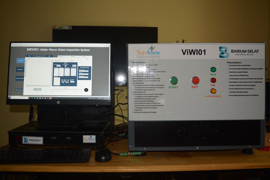
Phase 1 - Semi-conductor Automated Inspection with Machine Vision
The sequence of operation is this:
- Sequentially, pick-up the wafer from the cassette
- Inspect the wafer
- Record the data
- And unload & put the wafer in the respective tray.
The wafers inspected for this project were 6 inch circular silicon wafer. This system will be further integrated with automatic motion control in the upcoming release.
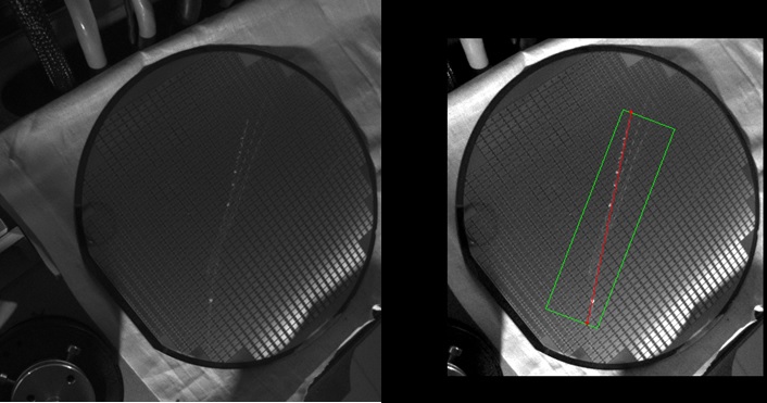
Some pictures of wafers are here -
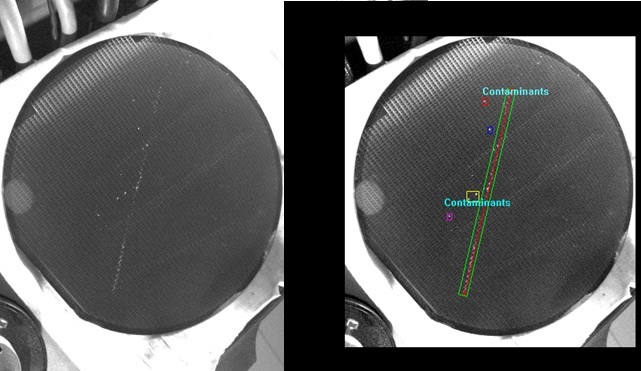
Showing contamination in wafer -
Housing Design - The housing consists of the following components:
- Top Clamp Mount: This is to clamp the camera as shown in Fig 1 in an inverted position from the top
- Ring LED Lights: There will 2 sets of Ring lights, each set consisting of 4 Ring Lights placed at four walls of the housing. As evident from Fig 1, the bright field Lighting sources are kept at a higher position than the dark field sources such that higher luminescence can be achieved by concentrating the light beam from all the sources in the wafer as opposed to dark field sources where the beam is diffused over the wafer.
- Wafer Placement Case: The case has been explained elaborately in section A.1
- Interface to Wafer placement case
Fig 1: Isometric Front View of Housing
A.1 Object Placer

Fig 2: Wafer Placement Case
A.2 Lighting Placement
Since the inspection of the wafers demands two types of lighting namely: Bright Field Lighting and Dark Field Lighting, there shall be two sets of light, each set consisting of 4 ring lights to be accommodated for emulating the Bright and Dark field. The Ring Lights are preferred to be of controllable gain and contrast such that the same light sources can be adjusted for different wafer surfaces.
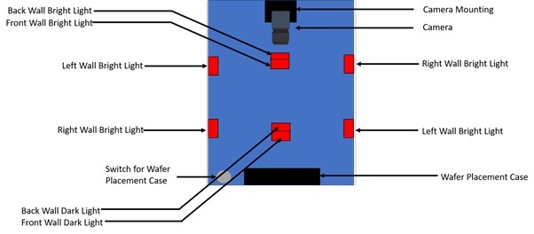
Fig 3: Isometric Front View of Lighting Sources
As seen in Fig 3, 2 sets of light sources are used placed at different positions in the wall. This is to maintain different angle of incidence of the light sources with respect to the wafer under inspection. The idea is to concentrate the light beam on the inspected wafer for achieving appropriate luminescence on the wafer without creating glare and distortion in case of bright field lighting. As can be seen in Fig 4, the beam is mostly concentrated on the object under inspection in case of bright field lighting and diffused in case of dark field lighting as can be seen in Fig 5. There shall be a simple strobe circuitry to switch between the Bright and Dark Light sources.
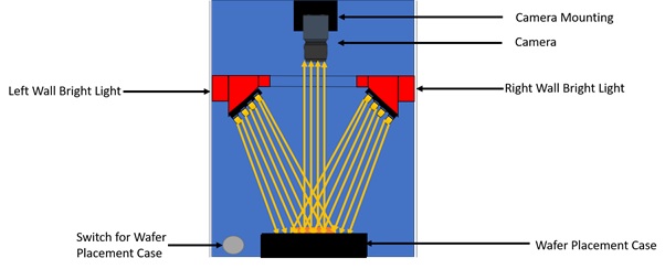
Fig 4: Bright Field Lighting
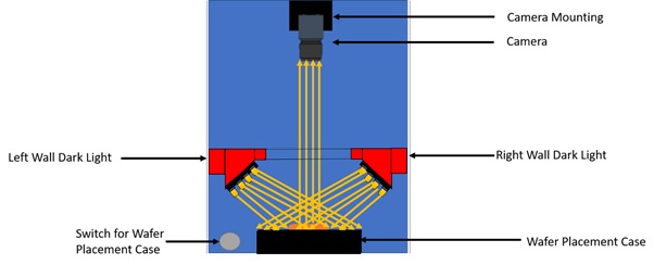
Fig 5: Dark Field Lighting
Main Measurements: Explanation of Main Measurements & Inspections with actual images captured by the frame grabber & processed by the machine vision algorithm.
Look and feel of the first version is here. We are offering automatic loading, flipping & unloading from cassette containing wafers in the upcoming version.
These images are for giving you an idea of the completed Phase 1.
Dies/Patches and Finger-prints: Detect dyes, patches and fingerprints and determine its location in active or passive region. Determine the individual dies and the total area encompassed.
Dies, Patches & Fingerprint on semiconductor wafers - automated detection using machine vision
U/V groove detection: Detect the presence of grooves and classify between U and V based on the magnitude of the mechanical cut. Get the width and length of the grooves.
U/V groove detection on semiconductor wafers - automated detection using machine vision
Detect surface scratches: Detect scratches and measure the length and area of the scratches
Scratches on semiconductor wafers - automated detection using machine vision
Automated OCR: Use our surface lighting solution for detecting and reading the Semiconductor Wafer ID based on Optical character recognition
Wafed ID on semiconductor wafers - automated OCR using machine vision
Wafer Measurements: Determine the diameter of the wafer and Flat edge radius
Diameter of semiconductor wafers - Diameter & flat edge radius automated measurement using machine vision
The test data from the software can be exported to Microsoft Excel or Microsoft Word. It consists of Time-Stamp, Batch-ID, Operator-Name, Wafer Diameter, Flat Radius, Serial-Number, Front Dye-Area, Scratch-Area, Length & Width of Front-Chip, Crack-Detected, Back Dye-Area, Back Scratch-Area, Metal-Ball-Count, Pass/Fail & Reason.
Please contact us using the form below or email from your company email ID for detailed explanation of the Algorithm for Inspection, video demonstration, presentation and quotation of the equipment.
